目录
1.算法运行效果图预览
2.算法运行软件版本
3.部分核心程序
4.算法理论概述
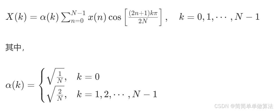
4.1 DCT离散余弦变换
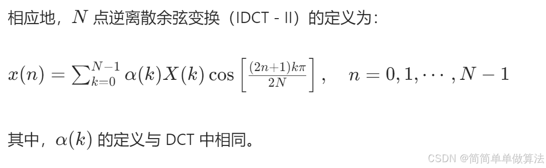
4.2 IDCT逆离散余弦变换
4.3 树结构实现1024点IDCT的原理
5.算法完整程序工程
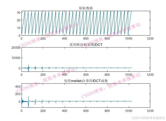
1.算法运行效果图预览
(完整程序运行后无水印)
matlab仿真结果
FPGA仿真结果
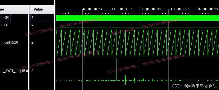
由于FPGA中的数据通常采用定点表示,在计算过程中会引入量化和舍入误差。因此,上述FPGA的测试结果,在数值较小时,和MATLAB存在一点误差。
2.算法运行软件版本
vivado2019.2
Matlab2022a
3.部分核心程序
(完整版代码包含详细中文注释和操作步骤视频)
`timescale 1ns / 1ps
//
// Company:
// Engineer:
//
// Create Date:    19:52:27 04/01/2014
// Design Name:
// Module Name:    myDD16
// Project Name:
// Target Devices:
// Tool versions:
// Description:
//
// Dependencies:
//
// Revision:
// Revision 0.01 - File Created
// Additional Comments:
//
//
module myDD16(x1,x2,x3,x4,x5,x6,x7,x8,x9,x10,x11,x12,x13,x14,x15,x16,Z1,Z2,Z3,Z4,Z5,Z6,Z7,Z8,Z9,Z10,Z11,Z12,Z13,Z14,Z15,Z16);input signed[15:0] x1;
input signed[15:0] x2;
input signed[15:0] x3;
input signed[15:0] x4;
input signed[15:0] x5;
input signed[15:0] x6;
input signed[15:0] x7;
input signed[15:0] x8;
input signed[15:0] x9;
input signed[15:0] x10;
input signed[15:0] x11;
input signed[15:0] x12;
input signed[15:0] x13;
input signed[15:0] x14;
input signed[15:0] x15;
input signed[15:0] x16;
output signed[15:0]Z1;
output signed[15:0]Z2;
output signed[15:0]Z3;
output signed[15:0]Z4;
output signed[15:0]Z5;
output signed[15:0]Z6;
output signed[15:0]Z7;
output signed[15:0]Z8;
output signed[15:0]Z9;
output signed[15:0]Z10;
output signed[15:0]Z11;
output signed[15:0]Z12;
output signed[15:0]Z13;
output signed[15:0]Z14;
output signed[15:0]Z15;
output signed[15:0]Z16;//STEP1
//STEP1
wire signed[15:0]s11_1;
wire signed[15:0]s11_2;
wire signed[15:0]s11_3;
wire signed[15:0]s11_4;
wire signed[15:0]s11_5;
wire signed[15:0]s11_6;
wire signed[15:0]s11_7;
wire signed[15:0]s11_8;assign s11_1 = x1 + x16;
assign s11_2 = x2 + x15;
assign s11_3 = x3 + x14;
assign s11_4 = x4 + x13;
assign s11_5 = x5 + x12;
assign s11_6 = x6 + x11;
assign s11_7 = x7 + x10;
assign s11_8 = x8 + x9;wire signed[31:0]s12t_1;
wire signed[31:0]s12t_2;
wire signed[31:0]s12t_3;
wire signed[31:0]s12t_4;
wire signed[31:0]s12t_5;
wire signed[31:0]s12t_6;
wire signed[31:0]s12t_7;
wire signed[31:0]s12t_8;
assign s12t_1 = (x1 - x16)*32610;
assign s12t_2 = (x2 - x15)*31357;
assign s12t_3 = (x3 - x14)*28899;
assign s12t_4 = (x4 - x13)*25330;
assign s12t_5 = (x5 - x12)*20788;
assign s12t_6 = (x6 - x11)*15447;
assign s12t_7 = (x7 - x10)*9512;
assign s12t_8 = (x8 - x9)*3212;wire signed[15:0]s12_1;
wire signed[15:0]s12_2;
wire signed[15:0]s12_3;
wire signed[15:0]s12_4;
wire signed[15:0]s12_5;
wire signed[15:0]s12_6;
wire signed[15:0]s12_7;
wire signed[15:0]s12_8;
assign s12_1 = s12t_1[29:14];
assign s12_2 = s12t_2[29:14];
assign s12_3 = s12t_3[29:14];
assign s12_4 = s12t_4[29:14];
assign s12_5 = s12t_5[29:14];
assign s12_6 = s12t_6[29:14];
assign s12_7 = s12t_7[29:14];
assign s12_8 = s12t_8[29:14];//STEP2
//STEP2
wire signed[15:0]Y1_1;
wire signed[15:0]Y1_2;
wire signed[15:0]Y1_3;
wire signed[15:0]Y1_4;
wire signed[15:0]Y1_5;
wire signed[15:0]Y1_6;
wire signed[15:0]Y1_7;
wire signed[15:0]Y1_8;
wire signed[15:0]Y2_1;
wire signed[15:0]Y2_2;
wire signed[15:0]Y2_3;
wire signed[15:0]Y2_4;
wire signed[15:0]Y2_5;
wire signed[15:0]Y2_6;
wire signed[15:0]Y2_7;
wire signed[15:0]Y2_8;
myDD8 U1(
.x1(s11_1),
.x2(s11_2),
.x3(s11_3),
.x4(s11_4),
.x5(s11_5),
.x6(s11_6),
.x7(s11_7),
.x8(s11_8),
.Z1(Y1_1),
.Z2(Y1_2),
.Z3(Y1_3),
.Z4(Y1_4),
.Z5(Y1_5),
.Z6(Y1_6),
.Z7(Y1_7),
.Z8(Y1_8)
);
myDD8 U2(
.x1(s12_1),
.x2(s12_2),
.x3(s12_3),
.x4(s12_4),
.x5(s12_5),
.x6(s12_6),
.x7(s12_7),
.x8(s12_8),
.Z1(Y2_1),
.Z2(Y2_2),
.Z3(Y2_3),
.Z4(Y2_4),
.Z5(Y2_5),
.Z6(Y2_6),
.Z7(Y2_7),
.Z8(Y2_8)
);//Reorder
//Reorderassign Z1=Y1_1;
assign Z3=Y1_2;
assign Z5=Y1_3;
assign Z7=Y1_4;
assign Z9=Y1_5;
assign Z11=Y1_6;
assign Z13=Y1_7;
assign Z15=Y1_8;
assign Z2={Y2_1[15],Y2_1[15:1]};
assign Z4=Y2_2-Z2;
assign Z6=Y2_3-Z4;
assign Z8=Y2_4-Z6;
assign Z10=Y2_5-Z8;
assign Z12=Y2_6-Z10;
assign Z14=Y2_7-Z12;
assign Z16=Y2_8-Z14;endmodule
23_019m
4.算法理论概述
在数字信号处理领域,离散余弦变换(Discrete Cosine Transform, DCT)及其逆变换(Inverse Discrete Cosine Transform, IDCT)扮演着重要角色。
4.1 DCT离散余弦变换
对于一个长度为 N 的一维离散信号 x(n),n=0,1,⋯,N−1,其 N 点离散余弦变换(DCT - II)定义为:
4.2 IDCT逆离散余弦变换
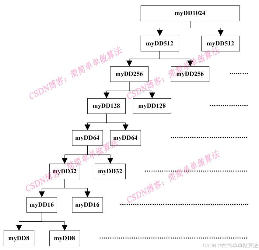
4.3 树结构实现1024点IDCT的原理
树结构实现 1024 点 IDCT 的核心思想是分治策略。将一个 1024 点的 IDCT 问题分解为两个 512 点的 IDCT 问题,每个 512 点的 IDCT 问题又可以进一步分解为两个 256 点的 IDCT 问题,以此类推,直到分解为 8 点的 IDCT 问题。
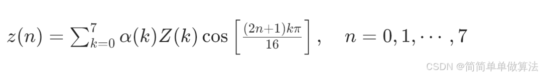
通过上述的结构,最终可以将问题归结为8点IDCT的计算。对于8点IDCT,设输入系数为Z(k),k=0,1,⋯,7,输出为z(n),n=0,1,⋯,7,其计算公式为:
具体来说,首先对输入的1024点IDCT系数进行分组,得到两个512点IDCT的输入系数;然后对每个512点IDCT的输入系数再进行分组,得到两个256点IDCT的输入系数,以此类推,直到得到多个8点IDCT的输入系数。接着,计算所有8点IDCT的结果;再根据这些结果计算256点IDCT的结果;然后根据256点IDCT的结果计算512点IDCT的结果;最后根据512点IDCT的结果计算1024点IDCT的结果。
5.算法完整程序工程
OOOOO
OOO
O
)

)


